Free One Week PCB Design Internship
Learn Schematic Design, 2D PCB Layout, 3D PCB Visualization and Gerber Generation with Cadence OrCAD & Allegro.
Start building real-world printed circuit boards in just one week — from electronics fundamentals to schematic design, layout, routing, Gerber generation and multilayer PCB design through live online sessions and practical work.
ஒரே வாரத்தில் PCB Design-ஐ practical-ஆக கற்றுக்கொள்ளுங்கள்.
Next PCB Design Internship Starts In
03.11.2026 – 10.11.2026 · 7:30 PM – 8:30 PM IST
Open to all degrees · Engineering & Non-Engineering · Beginners welcome
100% FREE
No registration fee
Registration Fee ₹0
LIVE ONLINE
Google Meet sessions
Live interactive training
PRACTICAL CADENCE
OrCAD + Allegro hands-on
Practical-ஆக PCB design
E-CERTIFICATE
Verified completion
Internship E-Certificate
What is the PCB Design Internship at Marcello Tech?
The One Week Internship Programme in PCB Design is a structured learning programme covering the complete PCB design workflow — from circuit schematics and PCB layout to 3D visualization and manufacturing file preparation. Programme dates, session details, and registration information are provided on this page.
Marcello Tech-ன் PCB Design Internship — circuit schematic முதல் manufacturing file preparation வரை முழு PCB design workflow-ஐ கற்றுக்கொள்ளுங்கள்.
Everything about your internship
உங்கள் Internship பற்றிய முழு விவரங்கள்
💻 Mode
100% Online – Google Meet
Live and interactive online sessions through Google Meet. Learn from home with real-time software walkthroughs, Q&A and practical assignments.
முழுமையாக Online-ல் Google Meet மூலம் Live Interactive Training நடைபெறும்.
📋 Programme Information
Key details at a glance
7 Training Sessions · Sunday 08.11.2026 Holiday
8 நாட்கள் காலண்டர், 7 training sessions. Sunday holiday.
Learn PCB Design by Doing Real Projects
This one-week internship programme is designed for students, beginners and electronics enthusiasts who want to master practical PCB design using industry-standard Cadence tools.
Theory மட்டும் இல்லாமல், Electronics Fundamentals + Schematic + Custom Footprint + Placement & Routing + Copper Pour + DRC + Gerber Generation + Multilayer PCB Design வரை 7 நாட்களில் practical-ஆக கற்றுக்கொள்ளுங்கள்.
// 7-Day PCB Engineering Workflow
1. Schematic capture in OrCAD Capture CIS
2. Custom Padstack & Footprint creation
3. Netlist export & Allegro import
4. Component placement & interactive routing
5. GND copper pour & thermal relief setup
6. Design Rule Check (DRC) verification
7. RS-274X Gerber & NC Drill manufacturing files
LAYERS
2 & 4 Layer
FORMAT
Gerber RS-274X
TOOL
Cadence 22.1
The Journey Your Board Takes
From circuit concept to a physical printed circuit board — explore the complete PCB design journey.
Circuit concept முதல் physical PCB வரை — முழு PCB design journey.
Stage 1
Schematic
Create the circuit diagram and define the electrical connections between components.
Circuit diagram உருவாக்கி component-களின் electrical connections-ஐ define செய்யவும்.
Ready to start your PCB design journey?
Register free for the One Week PCB Design Internship — 03.11.2026 – 10.11.2026.
High Demand in Embedded & Hardware Industry
Electronics, Embedded Systems, IoT, Automotive மற்றும் Consumer Tech துறைகளில் PCB Designers-க்கு அதிக வாய்ப்புகள் உள்ளன.
Industry Standard Software
Learn Cadence OrCAD & Allegro used by top MNCs, semiconductor companies and Tier-1 hardware R&D teams globally.
உலகளவிலான R&D நிறுவனங்கள் பயன்படுத்தும் Cadence OrCAD & Allegro கற்றுக்கொள்ளுங்கள்.
High Paying Core Jobs
PCB Layout Engineers, Hardware R&D Engineers and Embedded System Hardware Designers earn competitive salaries.
Hardware Design & Electronics R&D துறையில் அதிக சம்பளத்துடன் கூடிய Core Jobs.
Manufacturing Handoff Skills
Learn real manufacturing deliverables: Gerber RS-274X, NC Drill, Pick-and-Place XY and Bill of Materials (BOM).
PCB தயாரிப்புக்கு தேவையான Gerber, NC Drill மற்றும் BOM தயாரிக்கும் முறை.
Multilayer PCB Expertise
Gain confidence in 2-layer, 4-layer and multilayer stack-ups, internal power/GND planes and high-density routing.
2-Layer & 4-Layer Multilayer PCB வடிவமைப்பு மற்றும் routing முறைகள்.
Hardware Portfolio Project
Create your own complete schematic and PCB layout output files to present in technical interviews & college projects.
Resume மற்றும் Technical Interview-ல் காட்ட சிறந்த Hardware Project Portfolio.
Versatile Applications
Apply skills across Automotive ECUs, IoT devices, Robotics, Smart Home appliances, Medical electronics and Drone Hardware.
IoT, Automotive, Robotics மற்றும் Drone Hardware துறைகளில் பயன்படுத்தலாம்.
Skills you will master in 7 days
PCB Design-க்கு தேவையான அனைத்து முக்கிய Skills-ம் இங்கே கற்றுத்தரப்படும்.
Electronics Fundamentals
Voltage, current, resistance, Ohm's law, component symbols & datasheets
Schematic Design (OrCAD CIS)
Project setup, placing parts, wire buses, power symbols, ERC & annotation
Padstack & Footprint Creation
Through-hole & SMD footprints, DIP, SOIC, TQFP footprint drafting from datasheets
Netlist Export & Import
OrCAD to Allegro netlist generation, footprint mapping & rat's nest verification
PCB Board Setup & Placement
Board outline, mounting holes, placement rules, decoupling cap strategy
Interactive Routing & Vias
Trace width rules, 45-degree routing, via selection, shove/glossing
Copper Pour & Thermal Relief
GND polygon pour, copper balancing, thermal relief pads & island removal
DRC Checks & Error Correction
Spacing, clearance, short circuit checks and step-by-step DRC error fixing
Gerber & NC Drill Export
RS-274X layer mapping, drill file generation, verification in Gerbv viewer
BOM & Pick-and-Place
Generating Bill of Materials excel, SMT centroid XY files for assembly
Multilayer PCB Design
2 vs 4-layer stack-up, internal GND/Power planes, via stitching & layer transitions
Cadence Allegro 22.1 Tools
Hands-on mastery of industry leading Cadence PCB design software environment
8-Step Learning Journey
Electronics → Schematic → Footprint → Placement → Routing → Copper Pour → Gerber → Multilayer
Electronics
Components, Ohm's law, datasheet analysis
Schematic
OrCAD Capture CIS schematic & ERC check
Footprint
Padstack Editor & custom footprint drafting
Placement
Board outline & strategic component placement
Routing
Interactive track routing, vias & clearances
Copper Pour
GND pour shapes, thermal relief & DRC check
Gerber
RS-274X, NC Drill, BOM & Pick-and-Place
Multilayer
4-layer stack-up, internal planes & output
Inside the Circuit — Input to Output
Follow how signals enter an integrated circuit, travel through the circuit, and reach the output.
Signal எப்படி IC-க்குள் நுழைந்து output-ஐ அடைகிறது என்பதை பாருங்கள்.
Input Signal
Animated signal traces entering the PCB
Output Signal
Waveform visualization at output
Conceptual signal-flow visualization. Actual signal behaviour depends on the circuit design and components.
7-Day Practical PCB Design Syllabus
7 training sessions — ஒவ்வொன்றிலும் practical PCB design topics.
Note: Exactly 7 training days (Day 1 to Day 7) · Sunday 08.11.2026 Holiday.
7-Session Training Calendar
College / வேலை நேரத்துக்கு suitable ஆக evening session 7:30 PM – 8:30 PM.
Day 1 — Electronics Fundamentals & Schematic Design
7:30 PM – 8:30 PM
Day 2 — PCB Terminologies, Layers & Design Fundamentals
7:30 PM – 8:30 PM
Day 3 — Netlist Transfer & Custom Footprint Creation
7:30 PM – 8:30 PM
Day 4 — PCB Board Setup, Placement & Routing
7:30 PM – 8:30 PM
Day 5 — Copper Pour, DRC & PCB Optimization
7:30 PM – 8:30 PM
Sunday Holiday — No Class
—
Day 6 — Gerber Generation & Manufacturing Documentation
7:30 PM – 8:30 PM
Day 7 — Multilayer PCB Design: Complete Practical
7:30 PM – 8:30 PM
Learn → Practice → Design → Verify
ஒவ்வொரு step-லும் practical-ஆக learn செய்யுங்கள்.
Learn
Understand electronic circuits & Cadence OrCAD/Allegro workflows
Practice
Draft schematics & custom footprint symbols during live sessions
Design
Layout components, route traces & copper pour shapes
Verify
Run DRC checks & verify Gerber RS-274X manufacturing output
Who can join this PCB internship?
PCB design பற்றி முன் அனுபவம் தேவையில்லை. Beginners கூட இந்த programme-ல் join செய்யலாம்.
1 WEEK
Focused Internship
7 DAYS
Practical Learning
7:30 PM
Evening Sessions
100%
Online Google Meet
₹0
Registration Fee
E-CERT
On Completion
What You Will Be Able To Do
7-Day Internship முடிந்தவுடன் நீங்கள் என்ன செய்ய முடியும்?
Create & validate complete circuit schematics in OrCAD Capture CIS
Draft custom SMD and through-hole footprints using Padstack Editor
Transfer netlists smoothly from OrCAD into Allegro PCB Editor
Layout components strategically and route clean 2-layer PCB tracks
Create GND copper pour shapes and solve thermal relief connections
Run Design Rule Check (DRC) and eliminate clearance & spacing errors
Generate production-ready Gerber RS-274X & NC Drill manufacturing files
Understand 4-layer multilayer PCB stack-up setup and internal planes
Ready to Design Your First PCB?
Join the free one-week PCB Design Internship and explore the complete design workflow.
PCB Design-ஐ basics முதல் Gerber outputs வரை கற்றுக்கொள்ளுங்கள். இன்றே உங்கள் registration-ஐ complete செய்யுங்கள்!
How registration works
Register Now click செய்த பிறகு வரும் form-ஐ முழுமையாக fill செய்து Submit செய்யவும்.
Click Register Now
Click the Register Free button anywhere on this page.
Register Now button-ஐ click செய்யுங்கள்.
Complete the Form
Fill in all required details in the PCB Design registration form and submit.
வரும் form-ஐ முழுமையாக fill செய்து Submit செய்யவும்.
Registration Confirmation
Your registration is processed and Google Meet details will be shared.
Form Submit செய்த பிறகே registration complete ஆகும்.
Real Students. Real Learning. Real Experience.
எங்கள் மாணவர்களின் உண்மையான Internship மற்றும் Training அனுபவங்களை பாருங்கள்.
What students say
மாணவர்களின் கருத்துக்கள்
"The PCB design sessions helped me understand schematic capture and footprint creation from absolute basics."
S1 — Marcello Tech Student
"I learned Cadence OrCAD Capture CIS and Allegro PCB Editor step by step through live practical walkthroughs."
S2 — Marcello Tech Student
"As a beginner in electronics, I was able to complete my first double-layer PCB layout and run DRC error checks."
S3 — Marcello Tech Student
"Generating real Gerber RS-274X files and NC Drill outputs gave me confidence to apply for hardware core jobs."
S4 — Marcello Tech Student
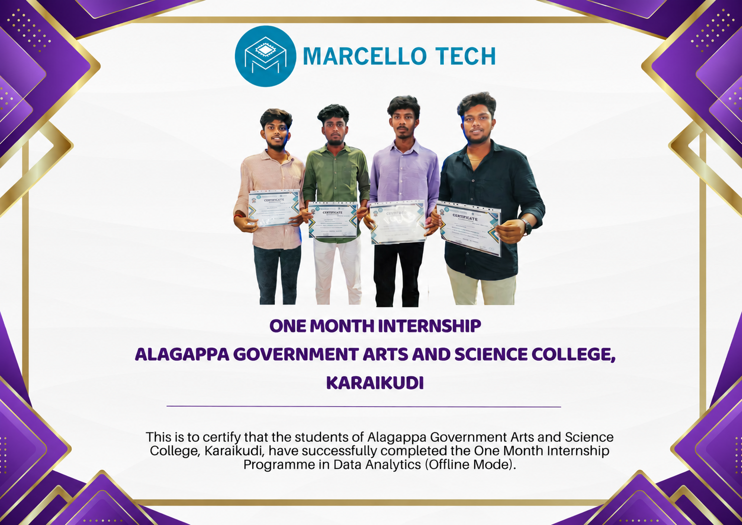
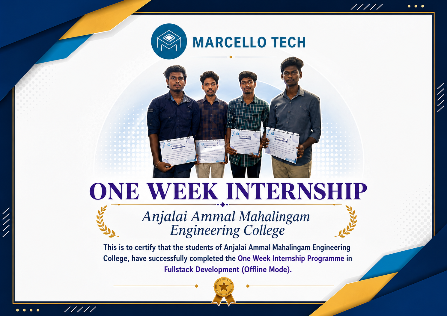
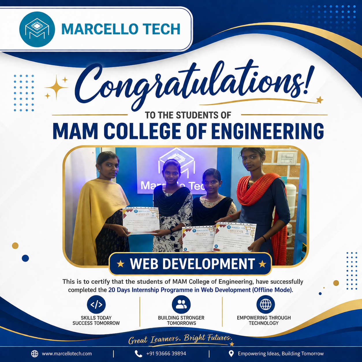
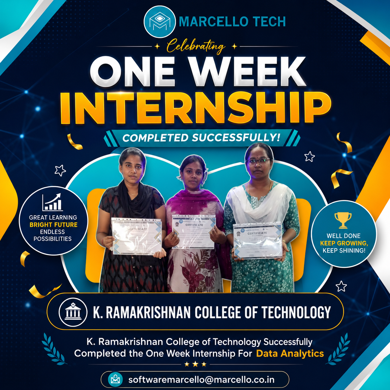
Complete the Internship. Earn Your Certificate.
Successfully complete the programme and receive a PCB Design Internship Completion E-Certificate.
Internship-ஐ முடித்தவுடன் உங்களுக்கான E-Certificate கிடைக்கும்.


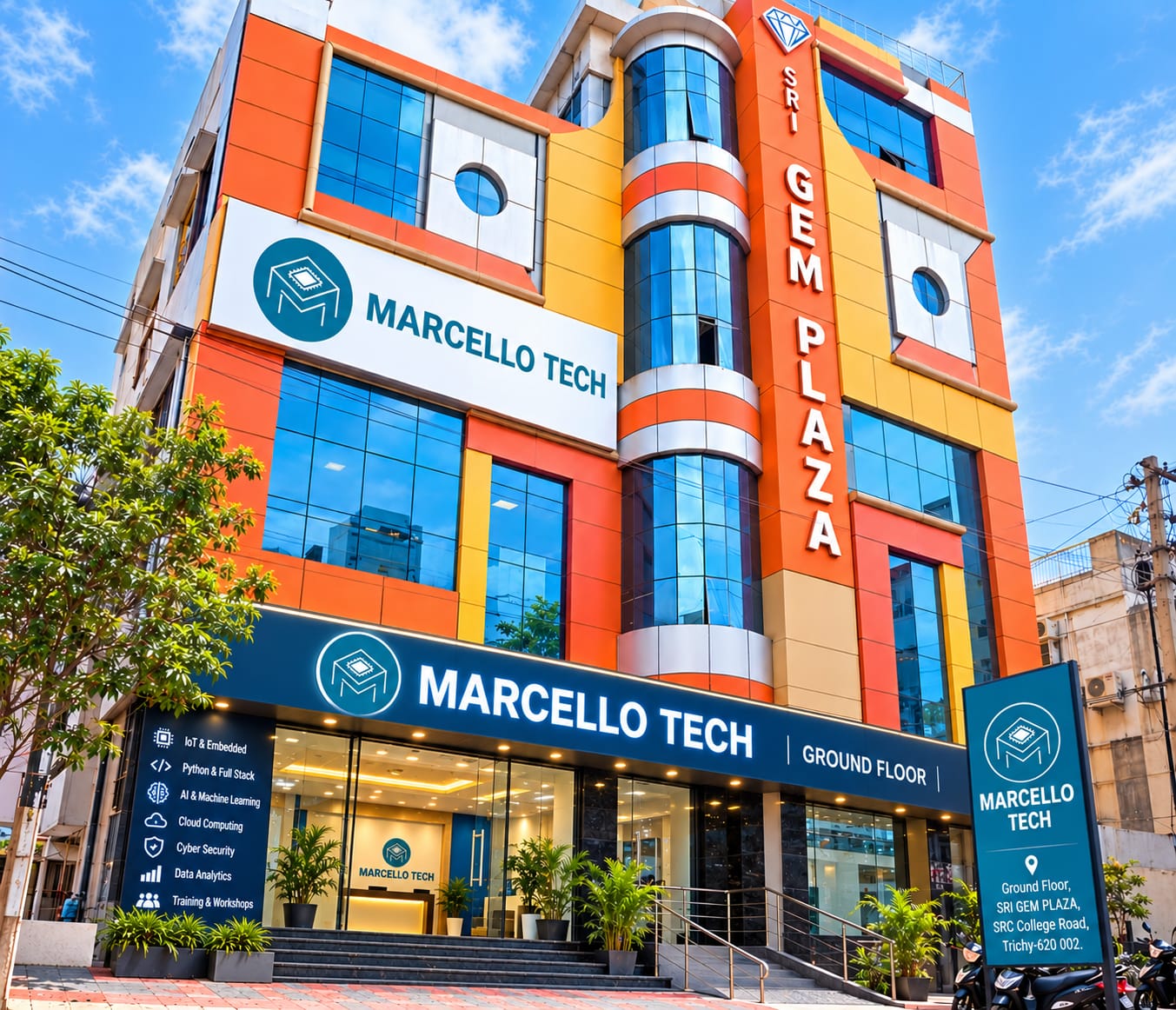
Visit Marcello Tech
Marcello Tech, Trichy-ல் உள்ள எங்கள் office-ஐ visit செய்யுங்கள்.
🏬 Marcello Tech
No. 3, GEM Plaza, Ground Floor,
Sankaran Pillai Road, Near Chathiram Bus Stand,
Trichy – 620002.
Frequently Asked Questions
அடிக்கடி கேட்கப்படும் கேள்விகள்
Your PCB Design Skills Start Here
Learn Cadence OrCAD & Allegro. Design Printed Circuit Boards. Gain Core Electronics Experience.
உங்கள் PCB Design learning journey-ஐ இன்றே தொடங்குங்கள்!
7 Training Sessions · 03.11.2026 – 10.11.2026 · Live Online · Google Meet · E-Certificate